Our goal is to establish ourselves as one of the most trusted digital VLSI design service providers in the industry. We aim to expand by cultivating key industry relationships and delivering cutting-edge solutions. By fostering a reputation built on transparency and seamless collaboration, we believe that teamwork is a cornerstone of our growth and success.

Our objective is to actively contribute to and promote the advancement of VLSI technology through all appropriate means. We consider our people to be our greatest asset, and we are committed to making a meaningful impact in everything we do.

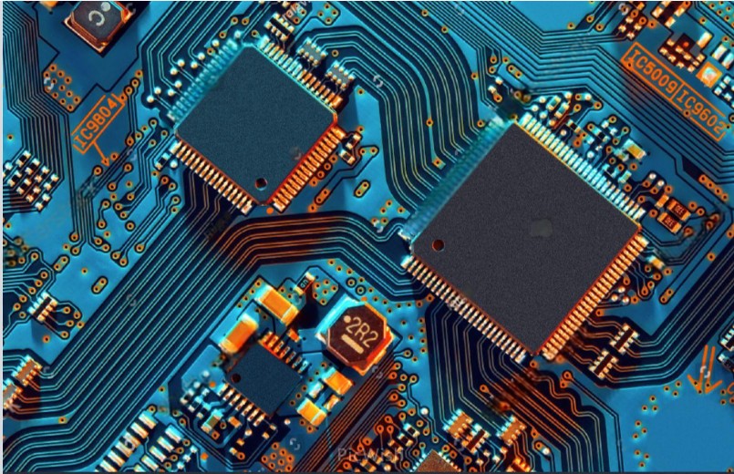
PD (Physical Design): SSSEMICON’s expert Team will provide support throughout RTL to GDSII stages of ASIC design flow. Our team has extensive experience in advanced flows for power aware synthesis (UPF, CPF), timing constraint generation (STA), netlist floor planning for best possible PPA and place and route(PNR) for overcoming ever increasing complexity. Our engineers in-depth knowledge of EDA tools and scripting skills enable us to deliver full turn-key ASIC development.
STA (Static Timing Analysis): is one of the most important area in Semiconductor chip Designing. Having an in-depth knowledge and exposure in STA provides opportunity in exploring and understanding how other domains operate to design chip. As expert say Timing and performance is almost everything, STA turns out to be the single most important domain which collaborates with every other areas of chip designing. SSSEMICON's Team can help to meet customer requirements and deliver as per expectations.
PV (Physical Verification): SSSEMICON’s verification team has proven expertise on taking complete ownership of verification. Verification is one of the key issues in IC design and development impacting the product schedules and timelines. We offer a wide range of ASIC verification services to help customers, especially physical verification checks like DRC, LVS, ERC, DFM, ESD, Antenna etc.
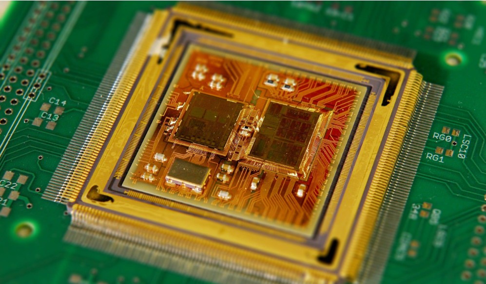
Analog Layout: SSSEMICON’s layout team has extensive experience in high speed and core analog layout. Our team has in-depth expertise on variety of IPs such as SerDes (10, 16, 30 & 56 Gbps), DDRphy, USB 2.0, MIPIphy and Power management. We have also handled expanded portfolios of Data converters, clock circuits such as PLL, DLL & oscillators, Regulators, Bias, Bandgap references, Temperature sensors, UVLOs etc SSSEMICON’s Team has proven experience on different process nodes to the cutting edge technology: Planar (180nm, 130nm, 110nm, 65nm, 55nm, 45nm, 40nm, 32nm, 28nm and more) and Finfet (16nm, 14nm, 12nm, 10nm, 7nm, 6nm, 5nm) with Foundry TSMC, Samsung, UMC, GF and Intel. Multiple full chip and IP level tape out has been successfully done with first pass.
Design Verification:SSSEMICON’s has one of industry’s strongest teams in design verification. Our team can execute verification from scratch of complex SoC’s and IPs by using latest methodologies such as SV-UVM, UPF and meeting key KPI such as 100% functional and code coverage Advanced IP & SoC Verification. We also provide silicon proven VIP for latest IP’s and provide source code and aftersales support to our customers.
RTL Design:SoC Architecture and IP Micro ArchSoC and Sub-System Integration, DFT RTL Design and Integration ,RTL Quality Checks, Synthesisi, Tming, Caliber and FEV ,Timing, Constraints and Constraints Validation